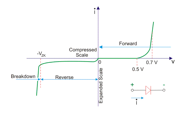
Draw the typical v i characteristics. A draw the circuit diagrams of a p n junction diode in i forward bias ii reverse bias.

Pn Junction Diode Characteristics Forward Bias External
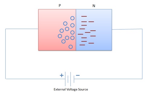
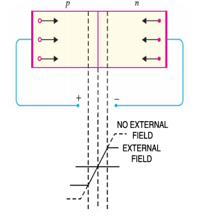
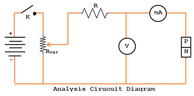
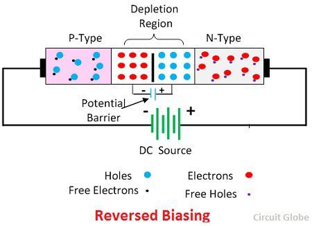
Pn junction diode forward and reverse bias circuit diagram. Keep in mind we are talking about a variable power source an ammeter in milli ampere range and a voltmeter. Fig2reverse biasing of p n junction diode this applied reverse voltage establishes an electric field which acts in the same direction as the field due to the potential barrier. As we have discussed that the diode is made of pn junction having one side of the p type material and another n type material. Hence the resultant field at the junction is strengthened and the barrier height is increased as shown in the above figure. B what is a light emitting diode led. When a junction diode is forward biased the thickness of the depletion region reduces and the diode acts like a short circuit allowing full current to flow.
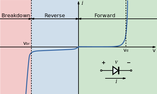
The biasing of a diode depends upon the direction of the source. In contrast to forward bias the reverse bias connection blocks the current passage and works as an open switch. Forward biased pn junction. How are these circuits used to study the v i characteristics of a silicon diode. When a junction diode is reverse biased the thickness of the depletion region increases and the diode acts like an open circuit blocking any current flow only a very small leakage current. Hence p n junction diode can be used as a rectifier.
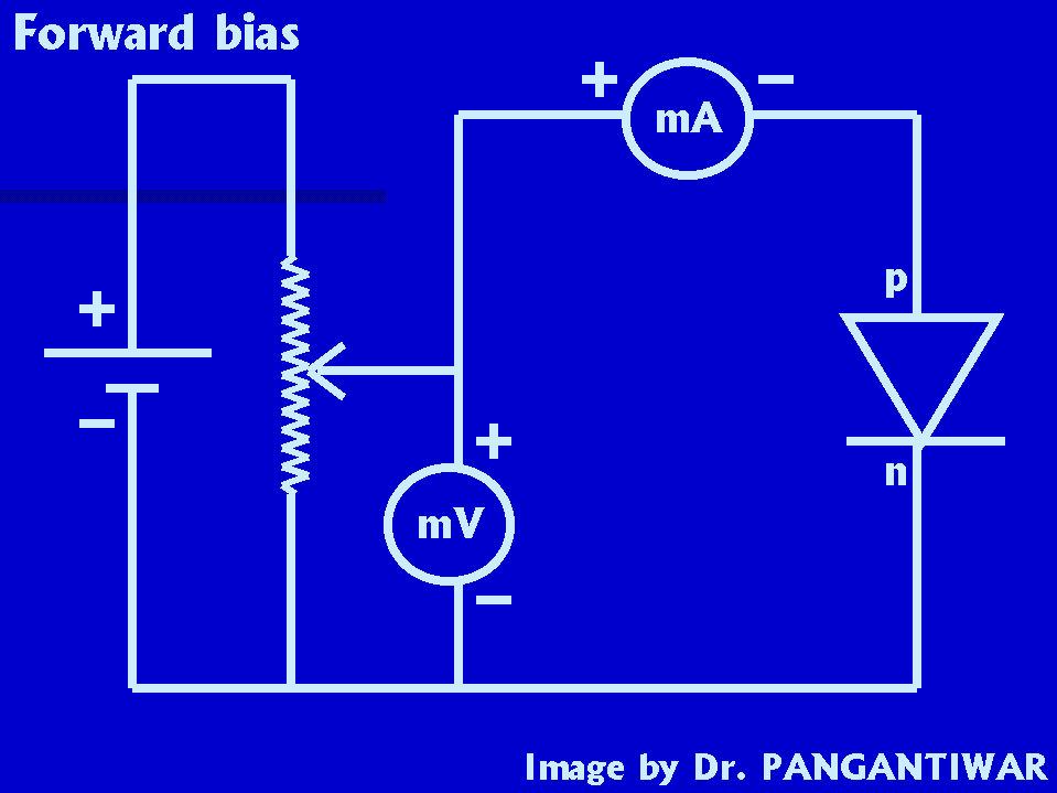
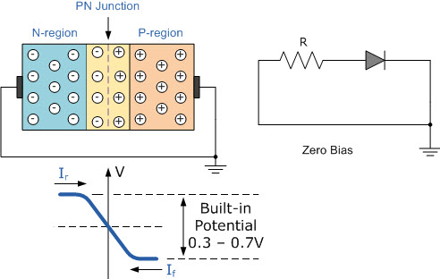
When we connect p type region of a junction with the positive terminal of a voltage source and n type region with the negative terminal of the voltage source then the junction is said to be forward biased. Lets get a voltmeter and ammeter and connect it to the forward biased circuit of pn junction diodea simple circuit diagram is shown below which has a pn junction diode a battery in picture it is not shown as variable. Mention two important advantages of leds over conventional lamps. Konduru madhava sarma physics for students 23741 views. When a diode is zero biased no external energy source is applied and a natural potential barrier is developed across a depletion layer. When the positive terminal of a battery is connected to p type semiconductor and negative terminal to n type is known as forward bias of pn junction.
At this condition due to the attraction of positive terminal of source electrons which participated in covalent bond creations in p type material will be. This process is known as rectification. P n junction forward bias and reverse bias in telugu for class 12. P n junction during forward bias offers low impedance path whereas during reverse bias acts as an insulator. Jee and neet duration. The p n junction diode during the reverse bias is highly sensitive to the light so that it can be used in photodiode application.
Gallery of Pn Junction Diode Forward And Reverse Bias Circuit Diagram