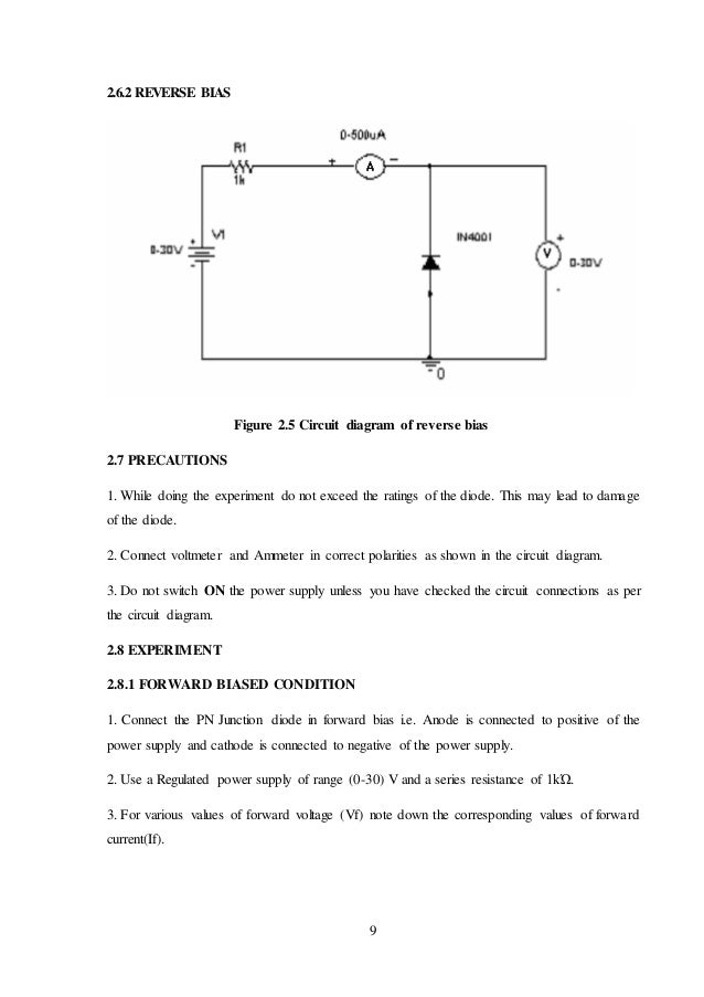
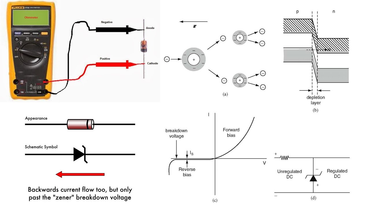
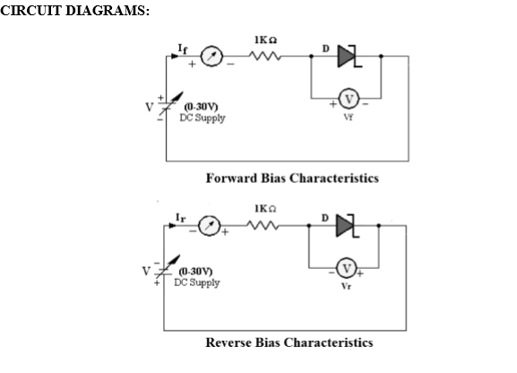
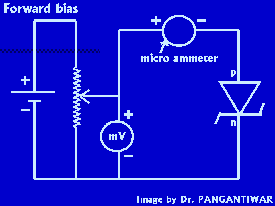
Lets get a voltmeter and ammeter and connect it to the forward biased circuit of pn junction diodea simple circuit diagram is shown below which has a pn junction diode a battery in picture it is not shown as variable. Zener diode connection characteristics of a zener diode.
Zener Diode Definition Working Principle
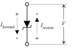
Zener diode forward and reverse bias circuit diagram. The essential difference between forward bias and reverse bias is the polarity of the voltage dropped across the diode. Some zener diodes have a sharp highly doped pn junction with a low zener voltage in which case the reverse conduction. The junction for the zener diode will be heavily doped. In contrast to forward bias the reverse bias connection blocks the current passage and works as an open switch. The forward bias reduces the potential barrier of the diode and establishes the easy path for the flow of current. When the diode is connected in forward bias diode acts as a normal diode.
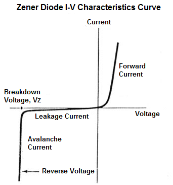
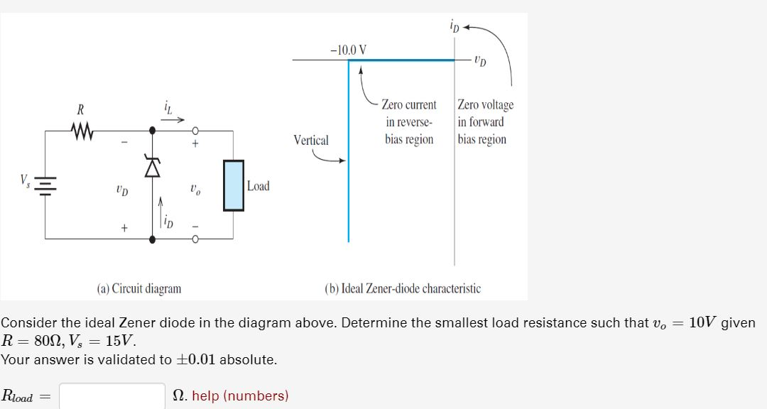
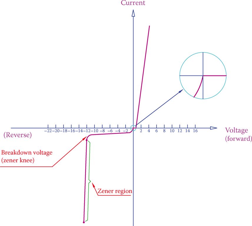
When the reverse bias voltage is greater than a predetermined voltage then the zener breakdown voltage occurs. A diode is two terminal electronics component which can be connected to the source in two different ways. The above diagram shows the v i characteristics of the zener diode behavior. The forward bias works like a closed switch and allows the current through itself. Working of the zener diode is similar to a pn junction diode in forwarding biased condition but the uniqueness lies in the fact that it can also conduct when it is connected in reverse bias above its thresholdbreakdown voltage. The special type of diode that can conduct in reverse bias is referred to as a zener diode.
Zener diodes are normal pn junction diodes operating in a reverse biased condition. A basic semiconductor diode can operate in forward bias but it cannot conduct during reverse bias. Zener diodes are manufactured with a great variety of zener voltages and some are even variable. While in reverse bias the potential difference increases the strength of the barrier which prevents the charge carrier to move across the junction. From the i v characteristics curve above we can see that the zener diode has a region in its reverse bias characteristics of almost a constant negative voltage regardless of the value of the current flowing through the diode. The diodes anode connects to the negative supply.
The graph shows the current vs voltage curve when we apply a reverse bias to the diode. Forward bias and reverse bias. This diode can conduct in forward bias just like a normal diode. Here in the diagram v z refers to the zener breakdown voltage. Lets take a closer look at the simple battery diode lamp circuit shown earlier this time investigating voltage drops across the various components in the figure below. The reverse bias provides the high resistive path to the flow of current and hence.
The zener breakdown voltage is the reverse bias voltage after which a significant amount of current starts flowing through the zener diode. Until the voltage reaches zener breakdown level tiny. The zener diode is used in its reverse bias or reverse breakdown mode ie. Keep in mind we are talking about a variable power source an ammeter in milli ampere range and a voltmeter. A zener diode is a special type of diode designed to reliably allow current to flow backwards when a certain set reverse voltage known as the zener voltage is reached. Diode circuit voltage measurements.
Gallery of Zener Diode Forward And Reverse Bias Circuit Diagram